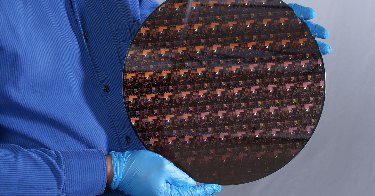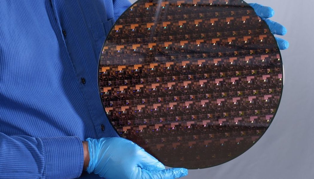
IBM has revealed what it says are the world’s first 2nm process chips, giving a brief preview of the technology that might eventually power the smartphones, laptops, and gadgets of the future.
The big jump here is in transistor count. Compared to today’s 7nm chips, the new IBM technology features dramatically more transistors, thanks to the more compact design. That means chips built using that process can potentially offer big gains in performance and battery life: IBM says its 2nm chips are “projected to achieve 45 percent higher performance, or 75 percent lower energy use, than today’s most advanced 7 nm node chips.”
According to AnandTech, IBM’s new 2nm chip features about 333 million transistors per square millimeter (MTr/mm2). For comparison, TSMC’s most advanced chips, built using its 5nm process, feature about 173 million transistors per square millimeter (MTr/mm2), while Samsung’s 5nm chips feature about 127 MTr/mm2.
While that all sounds great, it’s important to remember that IBM’s 2nm chip is largely just a proof of concept and that processors build on the 2nm node are still likely years away.
TSMC and Samsung, as mentioned before, produce 5nm chips right now. Intel is still struggling to get its 7nm node out the door. And even TSMC doesn’t expect to get to 2nm for some time: it’s currently planning to start early production of its 4nm chip process by the end of the year, with mass production in 2022, per AnandTech. Its 3nm node isn’t expected until the second half of 2022, with 2nm chips still in relatively early development. And all of that assumes that semiconductor companies don’t run into delays — just ask Intel, which has seen any number of manufacturing hiccups over the past decade or so.
Still, it’s a tantalizing glimpse at the future of semiconductor technology, and even though it may take some time to achieve on a mass-production scale, IBM’s announcement shows that there’s still plenty to be excited about when it comes to new chips.


